Building a computer from logic gates
Ever wondered how computers actually work on a low level?
After Jeff Atwood's recent post about Robot Odyssey, I did.
The following is a sketch of what could work, not necessarily what modern hardware actually does. The aim is to explore how a Turing-complete, multi-purpose computation engine could in principle be built from simple logic elements.
From silicon to computation
Nearly all chips are manufactured on silicon plates called wafers. These plates are modified in a complex process to create semiconductor-based diodes and transistors. Most general-purpose processors use a technology called CMOS that arranges the transistors into logic gates – devices that carry out operations on zeros and ones. The most common gate to implement is the NAND. All other common logic gates (AND, OR, NOT, XOR, ...) can be constructed from NAND building blocks.
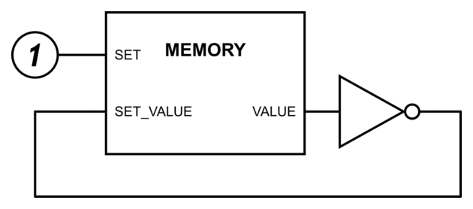
Memory cells can be constructed by composing multiple logic gates. Each cell stores a single bit of information. Conceptually, it has one output (VALUE) where the current value can be read. Additionally, there are two input pins: SET and SET_VALUE. For reading, SET is zero. For writing, SET is one and the SET_VALUE becomes the new value stored in the cell. It's not hard to imagine how to build a memory controller on top of an array of memory cells that allows addressing of individual cells for getting and setting their value.
How can memory be modified in practice? For example, how is it possible to invert (change 0 to 1 and vice versa) the value of a memory cell? Reading the memory, inverting it and writing it back into the memory cell leads to oscillation: when the cell value is changed it is immediately read back, and inverted and written again. This cycle repeats as quickly as the electronics can handle.

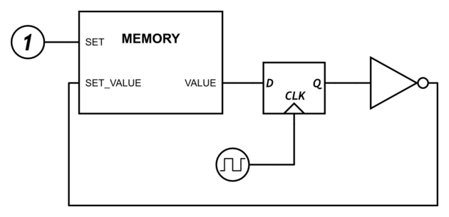
The solutions to this conundrum are clocks and edge-triggered flip-flops. Clocks are signals switching between 0 and 1 at a defined frequency. Edge-triggered flip-flops read their input at the rising edge of the clock (when it switches from 0 to 1) and output that value until the next rising edge. In other words, they sample their input once per clock cycle and hold that value until the next cycle. When such an element is inserted into the inversion loop, the memory value is inverted exactly once per clock cycle.

Based on this technique other operations can be implemented as well, such as adding or multiplying memory cells, copying memory contents to other locations, performing bitwise operations, and so on.
General-purpose processors
For each of those operations the logic gates would have to be arranged differently, though. In contrast, real general-purpose CPU's have fixed logic circuits, their gate configuration doesn't change during runtime. Instead, the operations to execute are read from memory and interpreted according to the chip's instruction set.
For our analysis, let's assume the command is read from separate input lines instead. We'll return to reading commands from memory later on.
How could one design and implement an instruction set? Let's say we have a machine with 8 lines (bits) of input and four 8-bit registers A, B, C, D. External memory is addressed in chunks of 8 bits and is attached via 8 address lines that select the location, 8 lines for reading/writing the 8-bit value, and one line to switch between reading and writing. What operations could we have?
| Opcode | Mnemonic | Description |
|---|---|---|
00RRVVVV |
SetHi VVVV, RR |
Set the 4 highest bits of register RR to VVVV. |
01RRVVVV |
SetLo VVVV, RR |
Set the 4 lowest bits of register RR to VVVV. |
1000RRSS |
Mov RR, SS |
Copy the value of register RR into register SS. |
100100RR |
Read [RR] |
Read from memory address stored in RR, store the result in register RR. |
100110RR |
Not RR |
Logically invert the value of register RR. |
100111RR |
Inv RR |
Negate (one's complement) the value of register RR. |
1010RRSS |
Add RR, SS |
Add registers RR and SS, store the result in SS. |
1011RRSS |
Mul RR, SS |
Multiply registers RR and SS, store the result in SS. |
1100RRSS |
And RR, SS |
Logical AND of registers RR and SS, store the result in SS. |
1101RRSS |
Or RR, SS |
Logical OR of registers RR and SS, store the result in SS. |
1111RRSS |
Write RR, [SS] |
Write the value of register RR to the memory address stored in register SS. |
It's not very efficient, but it enables a good amount of computation. How could it be implemented? All the separate opcodes could be realized as separate logic blocks on a chip. Each of them individually should be relatively easy to implement. Selecting which block to run (depending on the opcode) is a bit tricky. The easiest way to handle this is to run them all, but only enable output to the registers and memory for the single command that is desired by the input. On every cycle, all possible commands would be computed simultaneously, but only the desired one would be allowed to write to registers and memory. Is it efficient? No. Would it work? Yes.
Finally, we can address the problem of reading instructions from memory. Given the system described in the previous paragraphs, it shouldn't be too hard to add a separate component that reads instructions from memory and feeds it to this computation engine. The two components would communicate via an instruction-pointer register. The instruction set could be expanded to include (conditional) jumps, making the overall system Turing complete.
Conclusion
There are several small problems with what I've described, e.g. how to deal with instructions that consume multiple clock cycles, but all of them are solvable without too much trouble.
Thinking this topic is an interesting exercise. On the transistor level, it's hard to see how a real processor could ever be constructed from these primitives. Possible in principle – but hard to see how to do in practice. Three levels of abstractions above, after gates and memory cells there are suddenly memory blocks that are addressable via a parallel protocol. Every abstraction step is comprehensible, yet complexity is built up quickly. Two levels of abstraction further we suddenly have an 8-bit microprocessor.
It must have been an exciting opportunity to figure all of this out in the middle of the last century.